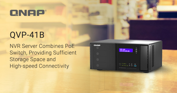
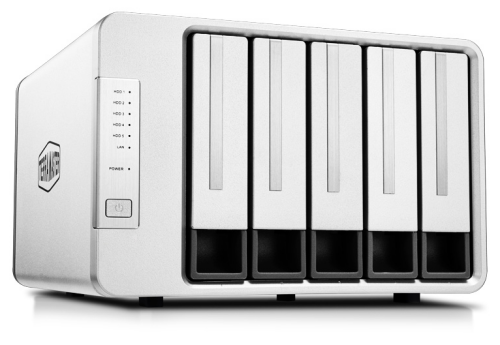
Synology Unveils Compact FlashStation FS2500 And latest SATA SSDs
Synology announced today the launch of FlashStation FS2500, the newest addition to the company's lineup of all-flash servers, as well as an update to its portfolio of SATA SSDs with SAT5210 drives.

Synology FlashStation FS2500: all-round storage platform for SMBs
The FS2500 is designed to tackle business IT applications requiring fast and low-latency storage, including virtual machines and post-production work. The compact, 1U chassis fits 12 2.5" SATA bays, providing ample capacity and simple installation.
"The new FS2500 addresses a growing demand for distributed computing," said Julien Chen, product manager at Synology. "The small footprint makes it a versatile solution that can be deployed at the edge or in mobile applications."
The unit delivers more than 170,000/82,000 4K random read/write performance, and features dual 10GbE ports with room for 10/25GbE expansion.
Add a comment

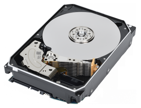
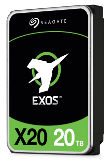 Data drives today’s most innovative technology and business breakthroughs. Maximizing the value of an organization’s data is dependent on the ability to store, access, and activate as much data as possible. Today, Seagate Technology Holdings plc, a world leader in mass-data storage infrastructure solutions, launched the new Exos X20 20TB and IronWolf ® Pro 20TB conventional magnetic recording (CMR)-based hard disk drives (HDDs), increasing mass-capacity data storage capabilities.
