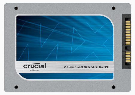
Crucial Announces Affordable MX100 SSD With 16nm NAND
Crucial, a leading global brand of memory and storage upgrades, announced today the new Crucial MX100 solid state drive (SSD). Available in 128 GB, 256 GB, and 512 GB capacities with respective MSRPs of $79.99, $109.99, and $224.99, the new Crucial MX100 offers powerful speeds and advanced features at a low cost per gigabyte.

The Crucial MX100 256 GB and 512 GB drives utilize Micron's new 16 nanometer (nm) 128 Gb NAND, in addition to a SATA 6 Gb/s controller and custom firmware, to deliver up to 90,000 input/output operations per second (IOPS). With true 550/500 MB/s sequential read/write speeds on both compressible and incompressible data, the Crucial MX100 allows users to boot up almost instantly, load programs in seconds, and accelerate demanding applications. Furthermore, at up to 89 percent more efficient than a hard drive, the new MX100 SSD allows users to run systems longer, using less power.


 Toshiba’s Digital Products Division (DPD), a division of Toshiba America Information Systems, Inc., today introduced the EXCERIA 1000x CompactFlash Memory Card, a versatile memory card that allows photographers to shoot and store more photos per second, enjoy smoother high-definition video, plus transfer or share images quicker and easier than ever before.
 Plextor, a leading developer of high-performance digital storage technology, announces the launch of M6 Pro and PlexTurbo at Computex 2014. The show will also mark the debut of other new consumer SSDs from Plextor, who will showcase their IPC and enterprise ranges.