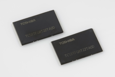
Toshiba Corporation today unveiled the new generation of BiCS FLASH, a three-dimensional (3D) stacked cell structure flash memory. The new device is the world’s first 256-gigabit (32gigabytes) 48-layer BiCS device and also deploys industry-leading 3-bit-per-cell (triple-level cell, TLC) technology. Sample shipments will start in September.

BiCS FLASH is based on a leading-edge 48-layer stacking process that surpasses the capacity of mainstream two dimensional NAND Flash memory while enhancing write/erase reliability endurance and boosting write speeds. The new 256Gb device is suited for diverse applications, including consumer SSD, smartphones, tablets and memory cards, and enterprise SSD for data centers.
Since announcing prototype BiCS FLASH technology in June 2007, Toshiba has continued development towards optimization for mass production. To meet further growth in the Flash memory market in 2016 and beyond, Toshiba is proactively promoting migration to BiCS FLASH by rolling out a product portfolio that emphasizes large capacity applications, such as SSD.
Toshiba has a long-standing commitment to flash memory, and is currently readying for mass production of BiCS FLASH in a new Fab2 at Yokkaichi Operations, its production site for NAND flash memories. Fab2 will be completed in the first half of 2016.

