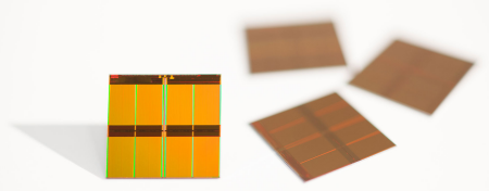
Micron Technology, Inc., today announced that it is sampling next-generation, 16-nanometer (nm) process technology, enabling the industry's smallest 128-gigabit (Gb) multi-level cell (MLC) NAND Flash memory devices. The 16nm node is not only the leading Flash process, but it is also the most advanced processing node for any sampling semiconductor device. It solidifies Micron's leadership position in storage technology development and delivers on the company's vision to provide the most advanced semiconductor solutions.

Micron's 128Gb MLC NAND Flash memory devices are targeted at applications like consumer SSDs, removable storage (USB drives and Flash cards), tablets, ultrathin devices, mobile handsets and data center cloud storage. The new 128Gb NAND Flash memory provides the greatest number of bits per square millimeter and lowest cost of any MLC device in existence. In fact, the new technology could create nearly 6TB of storage on a single wafer.
"Micron's dedicated team of engineers has worked tirelessly to introduce the world's smallest and most advanced Flash manufacturing technology," said Glen Hawk, vice president of Micron's NAND Solutions Group. "Our customers continually ask for higher capacities in smaller form factors, and this next-generation process node allows Micron to lead the market in meeting those demands."
"Cost reductions will always be fundamental to the NAND industry and so companies who can continue to lead on the flash process technology will be poised for success, particularly in vertically integrated solutions," according to Gartner.*
Micron is sampling the 16nm, 128Gb MLC NAND with select partners now and plans to be in full production in 4Q13. Micron is also developing a new line of solid-state drive (SSD) solutions based on these devices and expects to ship SSDs with 16nm Flash in 2014.

